Pentium 4 Block Diagram Explanation. Pentium 4 Block Diagram Pentium 4 Cache Operating Modes Note Pentium 4 Block Diagram Block Diagram Of The Pentium 4 Fo Basic Structure Of A Pentium Microprocessor Figure 1 From Comparison Of Intel Single Core And Intel Dual Intel Pentium 4xeon Nocona Intels Pentium D 820 And Pentium 4 670 Processors The. The middle of the diagram illustrates the out-of-order buffering logic and the bottom of the diagram shows the integer and floating-point execution units and the L1 data cache.
Its components are shown by the pictorial to be easily identifiable. Here is a basic explanation of each stage which explains how a given instruction is processed by Pentium 4 processors. Is the least efficient diagram among the electrical wiring diagram.
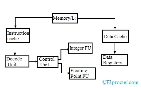
Pentium 4 block diagram.
Pentium 4 Block Diagram Explanation It is far more helpful as a reference guide if anyone wants to know about the homes electrical system. Here is a basic explanation of each stage which explains how a given instruction is processed by Pentium 4 processors. Technology has developed and reading Pentium 4 Block Diagram Explanation books might be far more convenient and simpler. Some of the features of Pentium architecture are.
